Since the first commercial scanning electron microscope came out in 1965, after 40 years of continuous improvement, the resolution of scanning electron microscopy has increased from 25 nm of the first one to 0.01 nm. Most scanning electron microscopy can be combined with X-ray spectrometer and X-ray energy spectrometer, which has become a comprehensive analysis of the surface micro-world. Multifunctional electron microscopy instrument. Scanning electron microscopy (SEM) has become a powerful tool widely used in various scientific fields and industrial sectors. Scanning electron microscopy (SEM) has been widely used in many fields, such as geology, biology, medicine, metallurgy, mechanical processing, materials, semiconductor manufacturing and ceramics inspection.
Scanning electron microscopy (SEM) plays an extremely important role in the field of materials. It is widely used in the study of morphology, interface condition, damage mechanism and material performance prediction of various materials. Scanning electron microscopy (SEM) can be used to study crystal defects and their production process directly. It can observe the aggregation mode of atoms in metal materials and their true boundaries. It can also observe the movement mode of boundaries under different conditions. It can also check the damage and radiation damage caused by crystal in surface machining.
Working Principle of Scanning Electron Microscope
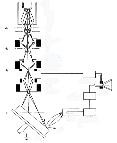
The working principle of the scanning electron microscope is shown in
Fig. 1 Scanning electron microscope schematic diagram
The scanning electron microscope (SEM) is composed of electron beams emitted from an electron gun. Under the action of accelerated voltage, the electron beams converge through a magnetic lens system to form an electronic optical system with a diameter of 5 nm. After two or three electromagnetic lenses, the electron beams converge into a thin electron beam focusing on the surface of the sample. A scanning coil is mounted on the upper side of the final lens, under which the electron beam is scanned on the surface of the sample. Due to the interaction between high energy electron beams and sample materials, various kinds of information are generated: secondary electrons, back-reflection electrons, absorption electrons, X-ray, Auger electrons, cathodoluminescence and transmission electrons. These signals are received by the corresponding receiver, amplified and sent to the gate of the picture tube to modulate the brightness of the picture tube. Because the current on the scanning coil corresponds to the brightness of the picture tube, that is to say, when the electron beam strikes a point on the sample, a bright spot appears on the screen of the picture tube. In this way, scanning electron microscopy (SEM) uses point-by-point imaging method to convert the different features of the sample surface into video signals proportionally in order to complete a frame of images, so that we can observe various characteristic images of the sample surface on the fluorescent screen.
Annex of Scanning Electron Microscope
Scanning electron microscopy (SEM) is usually equipped with a spectrometer or an energy spectrometer. The spectrometer uses Bragg equation 2dsin (= () to excite X-rays from the sample and to separate them by appropriate crystals. The characteristic X-rays with different wavelengths will have different diffraction angles of 2 (). Spectrometer is a powerful tool for micro-area component analysis. The wavelength resolution of the spectrometer is very high, but its application range is limited because of the low utilization of X-ray. Energy spectrometer is a method of element analysis based on the energy difference of X-ray quantum. For an element, when the X-ray quantum transits from the main quantum number stomach N1 to the main quantum number n2, there is a specific energy (=(n1-(n2). Energy dispersive spectrometer has high resolution and fast analysis speed, but its resolution ability is poor. There are often overlapping lines, and the accuracy of element analysis for low content is very poor.
Spectrometers and energy spectrometers can not replace each other, but complement each other.
Application of Scanning Electron Microscope in Material Science
Observation of Surface Morphology of Materials
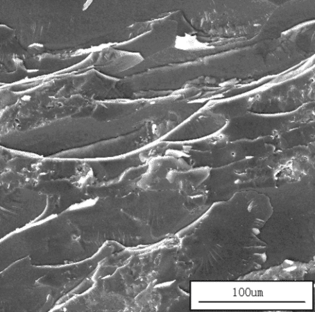
FIGURE 1 SEM MORPHOLOGY OF HOT ROLLED Mg SIDE PEELLING SURFACE
The SEM morphology of Mg side peeling surface of hot rolled Al-Mg clad sheet (rolling temperature 400 C, reduction rate 45%) is shown in Figure 1. From the graph, we can clearly see that there are a lot of tearing edges and platforms on the peeling surface, and there are many small radial stripes and dimples on the tearing platform.
Second Phase of Observing Material

Figure 2 High-power Microstructure of AZ31 Magnesium Alloy by SEM
It can be clearly seen from Fig. 2 that the size of the second phase Mg17Al12 after fragmentation is about 4 m, and there are many dispersed small particles near the “bulk” Mg17Al12 with the size of about 0.5 m. This is the second phase Mg17Al12 precipitated from the supersaturated solid solution of a-Mg base during the cooling process after hot rolling, showing the fineness of this morphological distribution. Biphasic Mg17Al12 can effectively inhibit dislocation movement, improve material strength and play the role of dispersion strengthening, but will not significantly reduce the plasticity of AZ31 magnesium alloy.
Observation of Material Interface
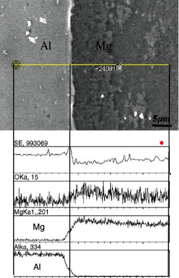
Figure 3 Mg/Al rolling interface line scanning [1]
Fig. 3 is a line scan image of Mg/Al rolling composite interface. From the graph, we can see that the line scan through the interface between Mg and Al can be obtained. On the Al side, the Mg content is low, and on the Mg side, Al is almost zero. However, at the interface, about half of Mg and Al occur, indicating that the diffusion occurs at the interface, forming Mg and Al. Diffusion layer.
Observation of material fracture
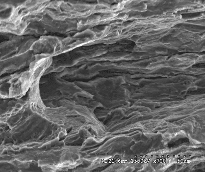
(a) As-cast
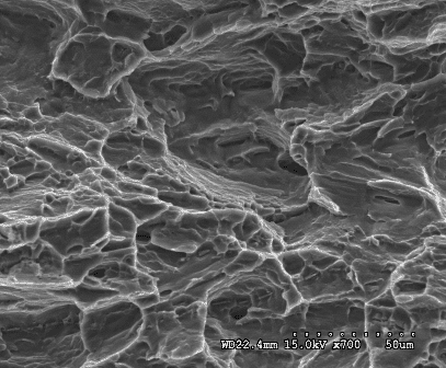
(b) Hot-rolled
Figure 4 Tensile Fracture Morphology of AZ31 Magnesium Alloy
The SEM scanning morphology of tensile fracture of as-cast AZ31 magnesium alloy is shown in Fig. 3-6. From Fig. 4 (a), it can be seen that there are obvious cleavage fracture platforms and a few dimples at the final tear point, which are basically quasi-cleavage fracture with poor plasticity. This is because there is a large brittle second phase Mg17Al12 at the grain boundary of as-cast AZ31 magnesium alloy, which is easy to crack and form crack source during tensile deformation. The fracture morphology of hot rolled AZ31 magnesium alloy shows obvious necking phenomenon. As shown in Figure 4 (b), the macro fracture morphology of AZ31 magnesium alloy shows ductile fracture morphology with dimple size ranging from 5 to 20 m.
Concluding remarks
Scanning electron microscopy (SEM) is widely used in material science. It can be used not only in the above aspects of material science, but also in fatigue failure of metals and morphological observation of impurities. As a student majoring in materials, we should understand the working principle and application of scanning electron microscopy, and make full use of the tool of scanning electron microscopy in our scientific research to conduct a comprehensive and meticulous study of materials.


